Given the complexity and the specific technical nature of a pinout diagram, creating one involves detailed technical drawing and annotation:
Interface Zones: Highlight zones for different interfaces (e.g., a section for memory, a section for PCIe).
Notes and Legend:
Include Technical Specifications:
Creating a detailed and accurate AM4 pinout diagram requires up-to-date technical specifications from AMD and involves careful planning to ensure that all features and functionalities are correctly represented. This process typically involves collaboration between hardware engineers and technical documentation specialists.
AMD AM4 socket features a Pin Grid Array (PGA) design with 1,331 pins
. Unlike Intel's LGA sockets, the pins are located on the CPU itself rather than the motherboard socket. AM4 Pinout Configuration Overview
The AM4 pinout is organized into a grid (typically labeled A-AM on one axis and 1-40 on the other) to handle power delivery, data transfer, and communication with peripherals. Key pin functional groups include:
Leo’s hands were shaking. Not from fear, but from the sheer density of what lay before him. Under the bright ring light of his workbench sat an AMD Ryzen processor, its underside a glittering field of 1,331 tiny gold contacts. Next to it, for the first time, he had unfolded the "AM4 Pinout Diagram"—a massive, multi-layered PDF that looked less like a technical drawing and more like a map of a subway system for a city built by ants.
“You’re staring at it like it’s a dead language,” Maya said, sliding a coffee next to his elbow. She was the hardware journalist; he was the overclocker. “It kind of is,” Leo replied. “This isn’t just power and ground. It’s a treaty.”
He zoomed in on the top-left corner. VDD and VDDCR_CPU. The lifeblood. Thick, red-coded lines on the diagram representing the main power delivery. “See these?” he tapped the screen. “If I short these to anything else, it’s not just a crash. It’s a funeral.”
Maya looked closer. The diagram was a symphony of colors. Yellow for the PCIe lanes—sixteen of them, plus four for the NVMe drive, all whispering directly to the processor like private phone lines. Blue for the DDR4 memory channels, twisted and paired so precisely that a single millimeter of trace length difference could cause a system to crash at 3600MHz.
“The story is in the holes, though,” Leo said, highlighting a cluster in the center. VSS. Ground. Dozens of them. “Ground pins aren't boring. They’re the foundation. Without this lattice of return paths, the high-speed signals would just bleed into each other.”
He traced a specific path with his stylus. SVI2—the power management bus. “This is the negotiator. The processor uses these two tiny pins to ask the motherboard for more voltage. ‘I’m about to boost to 4.8GHz, give me 1.35 volts.’ The motherboard’s VRM listens. That conversation happens in microseconds, right here.” am4 pinout diagram
The real drama, however, was in the RSVD pins. Reserved. On the diagram, they were gray voids. “Nobody knows exactly what AMD planned for these,” Leo whispered. “Some became the VDDG for the infinity fabric between the core chiplets. Others are just... silent. If you probe them with an oscilloscope, sometimes you see a heartbeat, sometimes nothing.”
He leaned back. The diagram wasn't a map of static metal. It was a biography of stress. The long VDDCR_SOC rail (System-on-Chip) was the hardest working pin, managing the integrated memory controller. If that pin got dirty power, the RAM would corrupt data. If a PROCHOT (processor hot) pin failed to pull low, the chip would literally melt itself trying to run Crysis.
“Look here,” Maya pointed. A tiny, lonely pin labeled ALERT#. “What’s that?”
“The watchdog,” Leo smiled. “When the CPU detects a fatal internal error—a ‘Machine Check Exception’—it doesn't crash immediately. It pulls that pin low to warn the motherboard’s BIOS. ‘I’m dying. Save the log.’ It’s the final whisper before the blue screen.”
Later that night, Leo built the machine. He didn't just drop the CPU into the socket. He visualized the dance. As he clamped the lever down, 1,331 springs compressed. The gold contacts of the processor kissed the pins of the motherboard. Power surged through the VDD arteries. The RESET# pin went high, releasing the CPU from its startup coma. The CLK (clock) pins began oscillating at 100MHz. And on the SVI2 bus, the first frantic negotiation for voltage began.
The screen posted.
“It’s alive,” Maya said.
Leo looked at the diagram one last time. “It was always alive,” he said. “We just couldn't see the conversation.” He folded the PDF away. The black box of silicon was no longer magic. It was a city, and he finally had the street map.
The AMD AM4 socket, also known as PGA1331, features a 1,331-pin layout and is the foundation for several generations of Ryzen processors . A good pinout diagram is essential for troubleshooting broken pins or understanding power delivery and data lanes. Core Pin Categories
VSS (Ground): The most common pins, often colored gray or black in diagrams. If you lose one of these, the CPU frequently still functions because of the high redundancy .
VDDCR_CPU (Core Voltage): These pins supply power to the CPU cores. Analysis of damaged chips often shows these as primary areas for thermal issues .
VDDCR_SOC: Provides power to the System-on-Chip (SoC) elements, including the integrated graphics and memory controller .
DDR4 Channels (MEM_): Groups of pins dedicated to communication with RAM (Channels A and B). Given the complexity and the specific technical nature
PCIe Lanes (P_GFX): Dedicated high-speed lanes for discrete graphics and NVMe storage .
Display Output (DP/HDMI): Pins specifically utilized by APUs (Ryzen chips with integrated graphics) to send video signals to the motherboard ports . AM4 Pinout Visualizations
Here are several diagrams and layout analyses of the AM4 socket: AM4 Socket Pinout Diagram | PDF
На процессоре ам4 нет контакта - 20.08.25 15:37 | Пикабу Пикабу
CPU pin broken off (AMD 5 5600 x, single pin, VSS) : r/techsupport
Demystifying the AM4 Pinout: A Guide for Ryzen Enthusiasts
If you’ve ever looked at the bottom of an AMD Ryzen processor and seen those 1,331 tiny gold pins, you’ve probably wondered what each one actually does. Whether you're trying to diagnose a "no post" issue or you’re staring in horror at a bent pin, understanding the AM4 pinout diagram is your first step toward a fix. What is the AM4 Pinout?
The AM4 socket (PGA 1331) uses a Pin Grid Array (PGA) where the pins are on the processor itself rather than the motherboard. A pinout diagram acts as a map, labeling each pin's specific function—such as power delivery (VSS/VCC), memory channels, PCIe lanes, or grounded pins. Why You Need a Pinout Map
Most users only look for a pinout when something goes wrong. Here are the most common scenarios:
Bent or Missing Pins: If you drop your CPU and a pin snaps, a pinout can tell you if it was a critical data line or a redundant ground pin.
Thermal Issues: Sometimes, specific pins related to power delivery can show signs of scorching if there’s a major voltage issue or socket failure.
Debugging: Advanced overclockers use pinouts to understand how voltage is supplied to the core versus the SOC. Key Sections of the AM4 Map
While the full diagram looks like a complex grid, it is generally divided into several zones: Interface Zones : Highlight zones for different interfaces
VSS (Ground): The most common pins. Many of these are redundant, meaning a single missing ground pin might not prevent the PC from booting.
Memory Channels: Pins dedicated to communicating with your DDR4 RAM. Damage here often leads to "single-channel only" memory issues.
PCI Express Lanes: These connect your CPU directly to your GPU and NVMe drives.
AZ_RST / Control: These are the critical "logic" pins that tell the system to start up. Helpful Resources for AM4 Diagrams
Finding an official "high-res" diagram can be tricky, as AMD doesn't always release these to the public. However, the community has filled the gap:
WikiChip: For a highly technical, interactive SVG map of the OPGA-1331 pinmap, WikiChip is the gold standard.
Community Forums: Platforms like Reddit r/Amd and the Level1Techs Forums often host user-made spreadsheets that categorize pins by color and function. Quick Tip: Dealing with a Bent Pin
If you find a bent pin, don't panic. Many users successfully use the "mechanical pencil" method or a thin credit card to gently nudge them back into alignment. Always check your AM4 pinout first to see if the bent pin is in a high-risk data zone or a safer ground zone.
Before diving into the diagram, it’s essential to understand the context. AMD launched the AM4 socket in 2016 to unify their entire consumer CPU lineup—from low-end A-series APUs (Bristol Ridge) to high-end Ryzen 9 chips. Unlike Intel’s LGA (Land Grid Array) sockets, AM4 uses a PGA (Pin Grid Array) design, where the pins are on the CPU itself. The motherboard socket consists of tiny holes with spring contacts.
This design choice makes the AM4 pinout diagram a CPU-centric map. If you flip your Ryzen processor upside down, the arrangement of pins follows a precise grid. Misplacing the CPU or bending a single pin can disconnect critical power delivery or memory channels.
The AMD AM4 (Socket AM4) platform, launched in 2016, represents a significant era in computing history. It served as the bridge between the traditional BIOS and modern UEFI environments and supported an unprecedented range of CPUs—from the entry-level Athlon to the high-core-count Ryzen 5000 series.
At the heart of this interchangeability lies the AM4 Pinout. With 1,331 pins arranged in a land grid array (LGA-style pads on the CPU, pins on the motherboard), the pinout defines the electrical pathways that allow the CPU to communicate with the rest of the system.
The vast majority of pins on the AM4 pinout are dedicated to power.


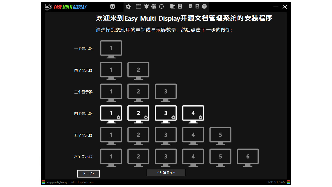
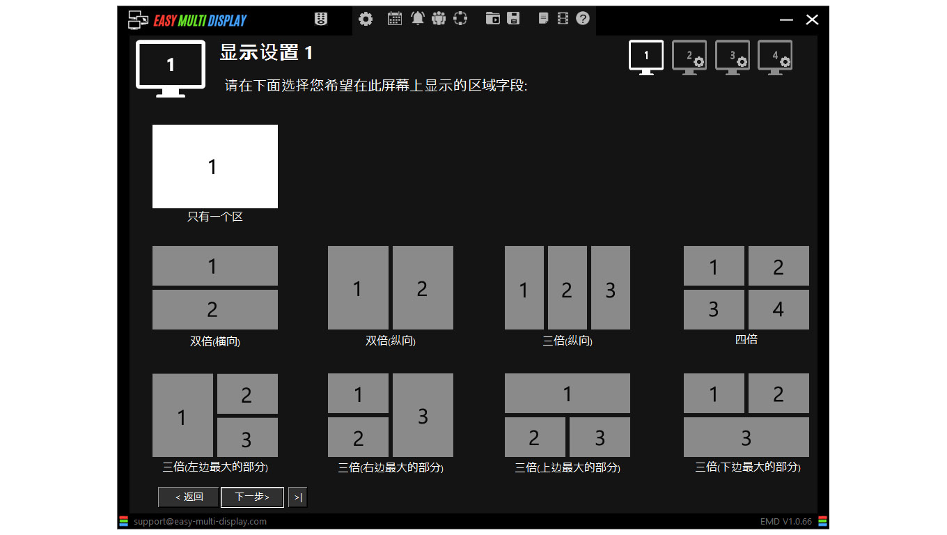
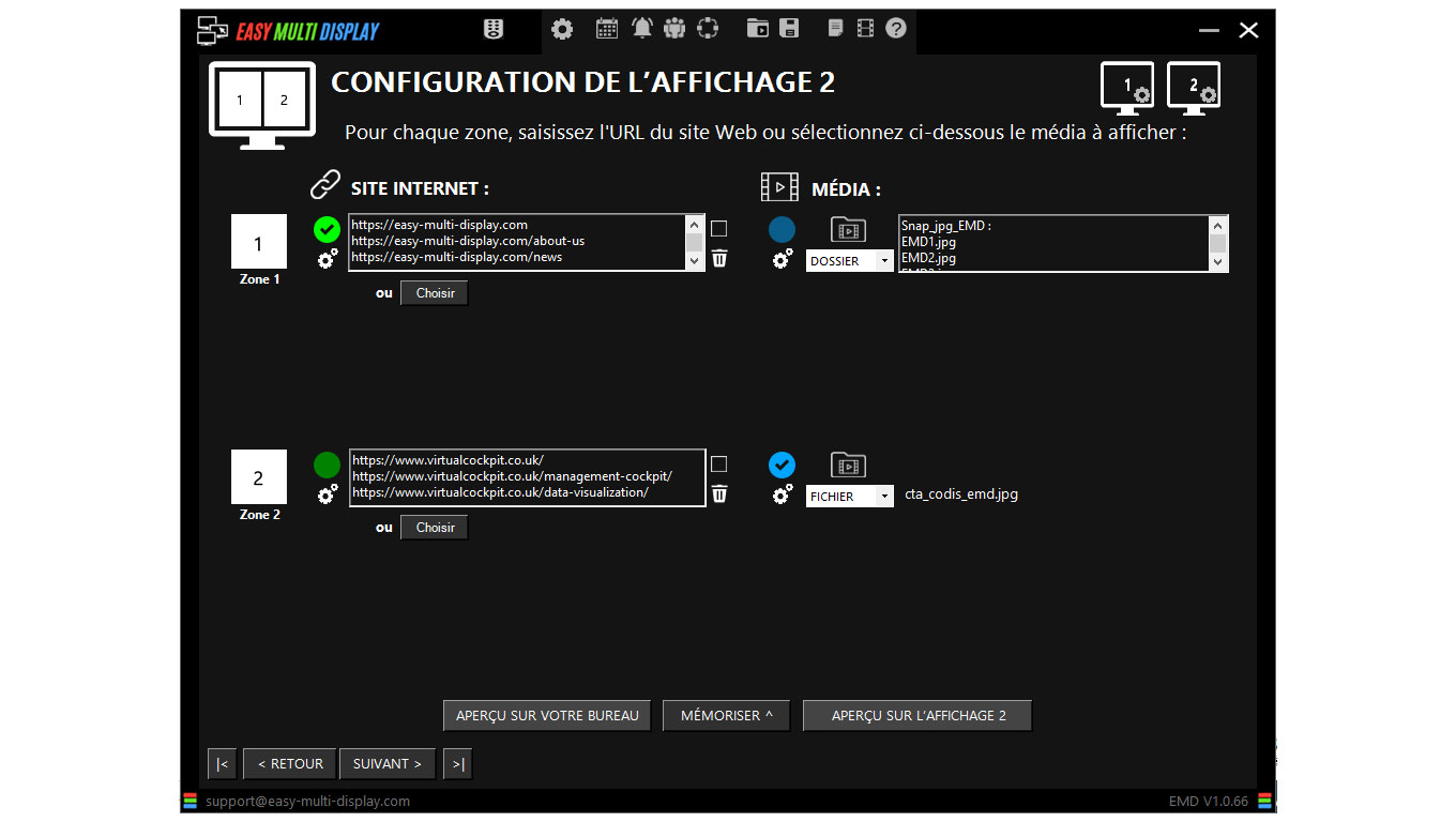
![Interview_Guy_Rave[pubs]_EasyMultiDisplay](https://easymultidisplay.com/wp-content/uploads/2023/02/Interview_Guy_Ravepubs_EasyMultiDisplay.jpg)